To follow this thread please keep an open mind; and don’t think you won’t understand it as I am going to keep it as simple as possible then at the end whether you followed it or not you will understand the conclusion even if you didn't see how it was reached.
My technical description may be a little outdated as I haven’t worked in this field for over a decade, but it should give you the idea. The greatest difficulty in reading this thread is that it is very logical, but needs to be followed letter for letter. I hope you have the staying power.
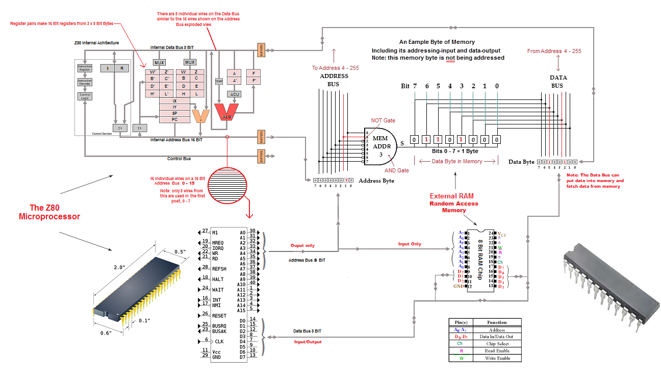
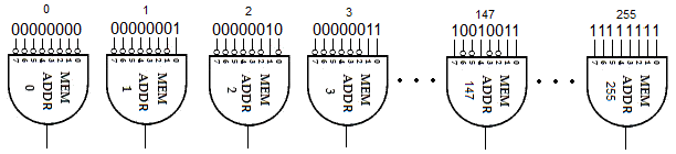
The next picture (Figure.1) is a simplified drawing of four bytes within a RAM chip...believe me four is enough…in the first part we are going to look at how we get the data out of one location, i.e. one byte of memory.

First I will explain the picture above. (It is assumed the reader understands binary notation). It is not necessary to understand the technology just try and follow the logic. We are going to talk about logic gates, if you can’t follow it then take this part of what I say for granted as it isn’t the point of this thread.
The "Black" lines represent wires that have no (or low) voltage representing a “0”, and the "Red" lines have a voltage representing a “1”. If it makes it easier, think of the “0” and “1” as “OFF” or “ON” respectively.
The D shapes with MEM ADDR (Memory address) written in them are “AND” gates, and a simple AND gate has two inputs, one output and works as follows:
Only if both the input lines are “1” {two in =D- one out} does the gate give an output of “1” else the output is “0”.
Now you can see in Figure.1 that these AND gates have eight inputs and only one output so to get the eight input configuration you need four AND gates together, but this gives four outputs and we only want one.
So a further two AND gates are placed in front of the four outputs giving two outputs, and one last AND gate is placed in front of these giving the one output that is required. This gives a configuration that looks like figure.2 below, and the D shape in fig.1 is a simplified representation of Figure.2. Follow it so far? Good

Remember that even the simple two input AND gate is only a representation. The circuitry for this can be seen in Figure 5 below.
In Fig.1, at the inputs to the AND gates you can see little circles, these represent “NOT” gates. A simple NOT gate has one input and one output and its function is to flip the input, thus if the input is “1” the output is “0” and vice versa. You can see the circuitry of the NOT gate in Figure 3. The circles in Fig.1 are simplified representations of this.

So now we are ready to extract our data…hopefully this is the easy bit to follow. 
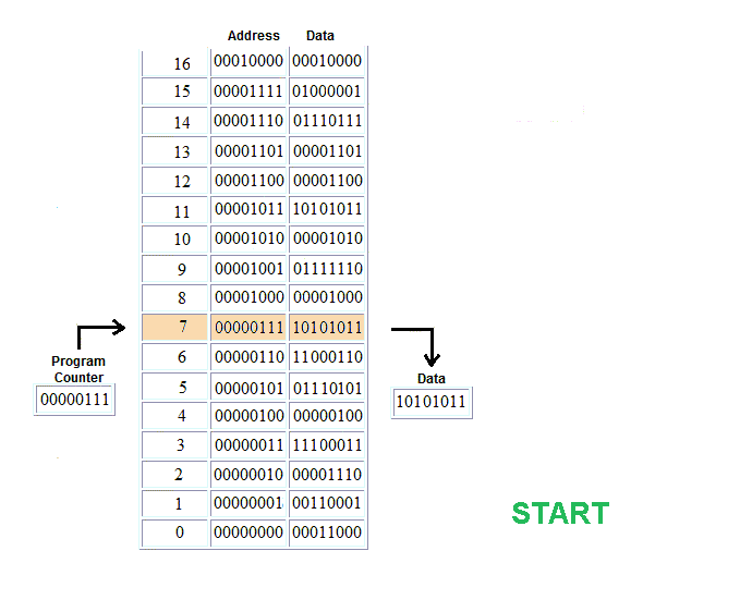
At the bottom of fig.1 you can see an address byte of memory – we won’t go into how that gets there…perhaps in another post lol – in this byte there is the binary number 00000010 which represents decimal 2 so we are addressing byte 2 of the RAM.
If we just follow the red line from the address byte we first come to Byte 0. You will notice that all inputs to Byte 0 have NOT gates so the AND gate sees all inputs as “1” except for the red line on input 1, which it sees as “0”, so the output is “0”, i.e. there is “0” on the “select” line for Byte 0.
Moving on we get to Byte 1. Here you will notice that all the inputs have NOT gates except for
input 0. Here the AND gate sees “1” on inputs 2 to 7, but “0” on inputs 0 and 1, so the output is “0”, i.e. there is “0” on the “select” line for Byte 1.
Now we get to Byte 2. Here you can see all inputs except input 1 have NOT gates and therefore the AND gate sees all these inputs as “1”, on input line 1 there is “1” and as this does not go through a NOT gate the AND gate sees this as “1” also. Now we have all inputs as “1” so the output is “1” and the Byte is selected. What happens next?
With the select line set to “1” this instructs the BIT cells in the byte to transfer their content onto the data lines and thus the content is received at the Data Byte…follow the red lines. You can now see that the Data Byte at the bottom of Fig.1 reflects the content of the data in Byte 2; Job done.
Note there is quite a bit that has been left out such as the read write line, which tells the Byte cells if they are putting data onto the data bus or retrieving data from it.
The Conclusion or The interesting bit.
Now we need to look at the circuitry of the previous components then the “AND gate” and the “BIT cells”; bear with me there is method in my madness.


OK looking first at Fig.3, The NOT gate, we can see it contains three components; two resistors R1,R2 and one transistor Q1; as the NOT gates will differ depending on the Byte Address I will average those at four per Byte which gives us twelve components.
Now looking at Fig.4, The SRAM BIT Cell contains six components; transistors M1 to M6, there are eight bits to a Byte therefore we have forty eight components.
On to Fig.5, The AND gate contains 10 components; four resistors R1 to R4, four transistors Q1 to Q4 and two diodes D1 and D2. Remember that was for a two input AND gate and we had to use seven to get our eight input AND gate, which gives us seventy components.
Now if we tally the number of components we need per Byte we come to 130 components.
The average RAM chip is 256Mbytes 256,000,000 Bytes so the components contained in one chip is… 33.28 Billion or… 33,280,000,000.
Now you do the maths, you can take the area of a chip – remembering that the chip is not what you actually see, the chip is inside a protective case, then divide that area by the 33.28 Billion and you get a rough idea of the size of the components we are manufacturing; obviously at the atomic level, but also probably at the quantum level today.
The address Byte we were using in figure one can address 256 addresses in memory, therefore we usually use a 16 bit address which allows 65,536 adresses. After this we can either page in different sections of memory and use the same 16 bits again (bit slow) or up the addressing to 32 bits which gives us 4,294,967,296 memory addresses or up it to 64 Bits which allows addresses up to 1.8447 x 10^19 memory addresses lol I'm not writing that one out.
So next time you hold a RAM chip in your hand be aware of the wonder you caress.
Hope you followed that…I’m sure there will be some that say they don’t use this or that lol, but it’s a good guestimate.
Thanks for staying with it.
Ghislain


.png)
.png)